
Samsung wants to fight with TSMC and Intel. Accelerated 2nm
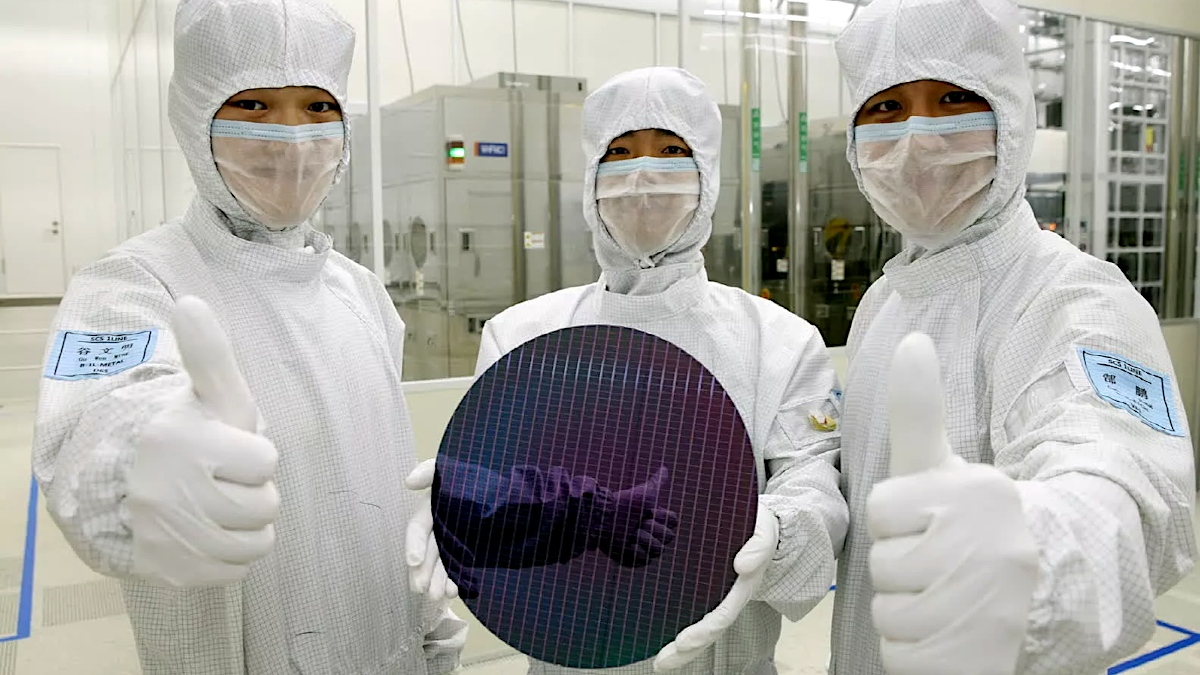
Samsung is getting closer to launching advanced semiconductor production in the USA. The latest reports indicate that the company will begin test operations of EUV machines in its factory in Taylor, Texas, in March. This is another step in the implementation of the plan to mass produce 2-nanometer GAA wafers on American soil.
FAB will be larger than those in South Korea
This facility will serve as a test bed for the installation, etching and deposition of key EUV equipment. Full-scale production is scheduled to start in the second half of 2026. For now, it is not known whether Exynos 2600 systems or other Samsung SoCs will be created in this location. However, it was confirmed that AI5 and AI6 chips for Tesla will be manufactured in Texas.
To speed up the work, 7,000 workers were employed at the construction site. After completion of the investment, the six-story building will accommodate approximately one thousand people. The sheer scale of the project is impressive. The area of the factory site in Taylor is 4.9 million m22making it larger than Samsung’s plants in Pyeongtaek and Hwaseong.
Europe is a major contributor to the latest lithographs
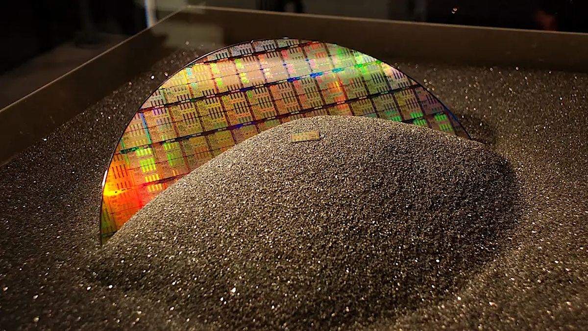
The key element of the whole puzzle are EUV machines from the Dutch ASML. Without them, mass production of 2nm GAA would be impossible. Currently, the efficiency of Samsung’s cutting-edge processes is estimated at around 50%, and improving this result is necessary if the company wants to bring its foundry business to profitability by 2027.
Costs remain an issue. One EUV machine costs approximately USD 339 million, or approximately PLN 1.2 billion. This poses a serious financial burden when Samsung posted total losses of up to $680 million in the third and fourth quarters of 2025.
On the other hand, the company showed foresight. The site in Taylor has been planned for the expansion of up to ten factories, leaving room for further expansion. Initially, this location was considered for production in 4 nm lithography, but in the face of TSMC’s reluctance to transfer the most advanced technologies to the USA, Samsung saw its opportunity. As a result, there is talk of an ambitious initial production target of 50,000 wafers, which may significantly strengthen the Koreans’ position on the global semiconductor market.


